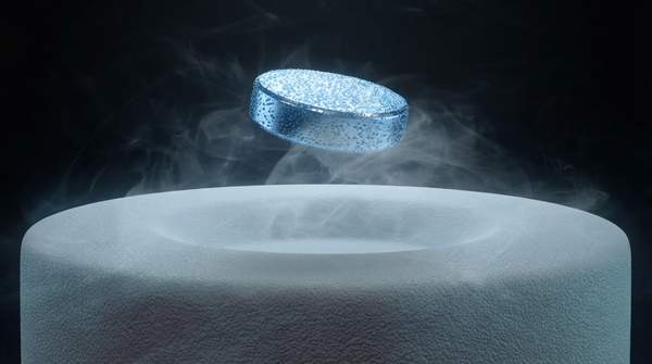
Quantum materials differ from ordinary matter in one decisive way: their macroscopic behavior is governed directly by quantum mechanics. Three classes dominate the field—superconductors, topological insulators, and quantum dots—and each is defined by a distinct quantum phenomenon. Superconductors carry current without energy loss, topological insulators conduct only along their surfaces, and quantum dots confine electrons so tightly that the color of their light emission can be tuned by size alone. Knowing which phenomenon defines each class is the key to understanding where each fits into future technology.
Introduction to Quantum Materials
What makes a material "quantum"? Oxford University's Department of Physics, whose research groups cultivate fresh compounds to study physical phenomena, treats superconductivity and magnetism as products of electronic correlations that can be adjusted by altering a material's composition. In other words, the quantum behavior emerges from how electrons interact inside the material, not just from what the material is made of.
This is the common thread across the classes we compare here. In superconductors, electrons work collectively so that current flows without resistance. In topological insulators, the geometry of the electron wave-function dictates where current can flow. In quantum dots, physical size itself becomes a design parameter. Each mechanism produces a signature property, and each property points toward a different application.
One caveat before we begin. This comparison covers three major classes, not an exhaustive catalog of quantum materials. The field also includes multiferroics—materials, as Oxford's physicists describe them, in which magnetic, charge, and elastic orders couple together—and other systems. Our goal is conceptual clarity about three classes a reader is most likely to encounter, not a complete taxonomy.
Superconductors: The Promise of Lossless Energy
Superconductivity is the clearest example of a quantum phenomenon operating at human scale. According to the U.S. National Science Foundation, the discovery of high-temperature superconductors—which carry electricity without energy loss while requiring less extreme cooling—sparked research into their unusual quantum behavior and its potential for practical technologies.
The appeal is obvious. Ordinary wires dissipate energy as heat; a superconductor does not. The catch is temperature. Even "high-temperature" superconductors require cooling, which is why the NSF describes the field as exploring their "potential" for practical technologies rather than delivering them. The less extreme the cooling required, the closer these materials move toward everyday use in power transmission and electronics.
It is worth being precise about what the evidence supports. The zero-resistance, lossless-carrying property is specifically documented for high-temperature superconductors, the family discovered in the late twentieth century that operates with less extreme cooling than earlier superconductors required. The NSF account does not enumerate specific applications; it frames the lossless property as the foundation on which practical technologies are being explored.
Topological Insulators: Protected Surface States
Topological insulators are stranger. Stanford's Shen Laboratory describes them as a newly discovered state of quantum matter: their interior is insulating, but their surfaces conduct electric current with a well-defined spin texture. They are classified not by conventional phase-transition theory but by a topological quantity in the electron's wave-function called the Chern number.
Why does this matter? Because the conduction lives on the surface and is tied to the material's topology, it is exceptionally stable. A 2026 University of Geneva study, led by senior research associate Giacomo Sala, worked with an antimony-tellurium compound described as "one of the most extensively studied topological insulators to date," with applications the team calls "highly promising." The Geneva work, focused on better control of the electrical properties of next-generation materials, illustrates how actively this class is still being characterized.
The Shen Laboratory notes that these materials can produce striking phenomena such as quantum spin Hall and quantum anomalous Hall effects, and even Majorana fermions—particles that are their own antiparticle—when placed near a superconductor. An early experimental review by Zahid Hasan and co-authors adds that their topological order can be realized at room temperature without magnetic fields, and that they can be turned into magnets and exotic superconductors. These properties make them candidates for spintronics and quantum computing.
Quantum Dots: Tunable Properties by Design
Quantum dots are the most tangible case study in how a quantum effect becomes an engineering tool. They are nanometer-sized semiconductor crystals, typically 1 to 10 nanometers across, made from groups II–VI and III–V elements. According to a review by Rajat Kumar Goyal and colleagues in the Journal of Materials Science, their defining phenomenon is quantum confinement: electrons and holes are squeezed into a volume so small that their energy levels become discrete.
The mechanism works like this. When an electron absorbs a photon and jumps to a higher energy state, it leaves behind a positively charged "hole." The electron and hole can bind into a quasi-particle called an exciton. Confinement kicks in when the exciton's natural size becomes comparable to or larger than the nanocrystal itself, forcing the energy levels into discrete steps rather than a continuous band.
The consequence is remarkable: smaller dots have larger energy gaps and emit higher-energy, bluer light, while larger dots emit lower-energy, redder light. Size literally sets the color. This tunability translates into practical advantages over organic dyes for bioimaging: wide absorption spectra, narrow emission spectra, lower photobleaching, and high quantum yield, allowing multiple targets to be tracked simultaneously. Each dot also has a core-shell structure, with the reactive core and stabilizing shell together offering better optical features and reduced toxicity.
Comparative Overview of Quantum Material Classes
The table below maps each class to its defining quantum phenomenon, the property that results, and the applications that follow. The pattern to notice: the phenomenon determines the property, and the property determines the use.
| Material Class | Defining Quantum Phenomenon | Key Property | Potential Applications |
|---|---|---|---|
| Superconductors | Superconductivity: zero electrical resistance | Carry electricity without energy loss (high-temperature superconductors, with less extreme cooling) | Practical technologies under exploration, including lossless power transmission |
| Topological insulators | Topological order: surface states classified by the Chern number | Insulating bulk with conductive, spin-textured surfaces | Spintronics and quantum computing |
| Quantum dots | Quantum confinement: electrons and holes restricted to a nanoscale volume, producing discrete energy levels | Size-tunable optical and electronic properties; smaller dots emit bluer light, larger dots emit redder light | Bioimaging and display technologies |
Read down the middle column and the differentiation becomes clear: zero resistance, protected surfaces, and tunable confinement are three entirely different answers to the question of how quantum mechanics can be engineered into a material. No one class substitutes for another—each solves a different problem.
The Future of Quantum Materials in Technology
Where do these classes converge? Quantum computing is the shared destination. Topological insulators offer robust surface states and, near a superconductor, can host Majorana fermions of interest for fault-tolerant quantum hardware. Superconductors supply the lossless currents and exotic phases that quantum circuits demand. Quantum dots, meanwhile, already deliver working optical tools in bioimaging today.
A caveat on expectations: these applications are largely potential or in development, not mature commercial products at scale. The NSF frames superconductor applications as exploratory; the Geneva team calls topological-insulator applications "highly promising" rather than realized. The physics is established; the engineering is still catching up.
Navigating the Quantum Frontier: Key Takeaways for Future Technology
To leverage the unique properties of quantum materials, researchers and developers should focus on understanding the specific quantum phenomena that define each class to unlock their full potential in next-generation technologies. The decision rule is simple: match the phenomenon to the task. Need lossless current? Superconductivity. Need robust, spin-controlled conduction? Topological protection. Need tunable light? Quantum confinement.
The measurable indicator of progress is continued advancements in material synthesis and characterization techniques, leading to the development of new devices utilizing these quantum properties. Watch for that signal: each new device built on zero resistance, protected surface states, or size-tuned emission marks concrete movement from quantum physics into working technology.
Sources
- Quantum materials — University of Oxford Department of Physics
- Engineering materials for the quantum age — NSF - U.S. National Science Foundation
- Topological Materials — Shen Laboratory
- The strange quantum property of tomorrow's insulator — Phys.org
- A new experimental approach for the exploration of topological quantum phenomena — arXiv.org
- API
- Exploring quantum materials and applications: a review - Journal of Materials Science: Materials in Engineering — SpringerLink